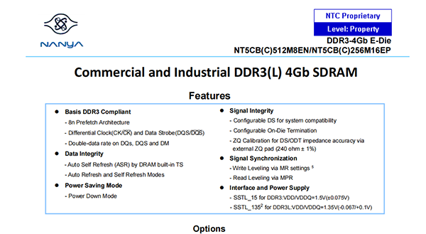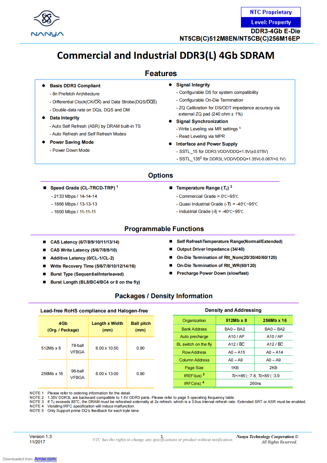

Basis DDR3 Compliant
-8n Prefetch Architecture
-Differential Clock(CK/)and Data Strobe(DQS/)
-Double-data rate on DQs,DQS and DM
Data Integrity
-Auto Self Refresh(ASR)by DRAM built-in TS
-Auto Refresh and Self Refresh Modes
Power Saving Mode
-Power Down Mode
CAS Latency(6/7/8/9/10/11/13/14)
CAS Write Latency(5/6/7/8/9/10)
Additive Latency(0/CL-1/CL-2)
Write Recovery Time(5/6/7/8/10/12/14/16)
Burst Type(Sequential/Interleaved)
Burst Length(BL8/BC4/BC4 or 8 on the fly)Programmable Functions
Self RefreshTemperature Range(Normal/Extended)
Output Driver Impedance(34/40)
On-Die Termination of Rtt_Nom(20/30/40/60/120)
On-Die Termination of Rtt_WR(60/120)
Precharge Power Down(slow/fast)
Signal Integrity
-Configurable DS for system compatibility
-Configurable On-Die Termination
-ZQ Calibration for DS/ODT impedance accuracy via external ZQ pad(240 ohm±1%)
Signal Synchronization
-Write Leveling via MR settings 5
-Read Leveling via MPR
Interface and Power Supply
-SSTL_15 for DDR3:VDD/VDDQ=1.5V(±0.075V)
-SSTL_1352 for DDR3L:VDD/VDDQ=1.35V(-0.067/+0.1V)